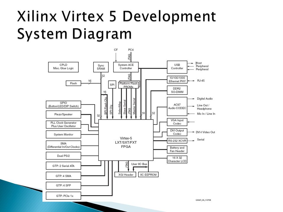
Virtex 5 Block Diagram
Virtex 5 Wiki Evariste
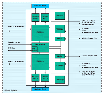
Designing With Virtex 5 Embedded Tri Mode Ethernet Macs

15 Virtex 5 Clb Block Diagram 18 Download Scientific Diagram

Vcc33 vcco0 vcc3en vcctmp vcco0 vcc33 vcco0.
Virtex 5 block diagram. One reference system is based on the powerpc 440 ppc440 processor and the other reference system is based on the microblaze processor. 29 art pn 0531591 fab pn 1280403 sch pn 0381232 schem rohs compliant virtex 5 ff1760 daughter 01 b. Supports endpoint to root complex dma full duplex read and write transactions initiated by. The reference design runs on the virtex 5 fpga ml555 development board for pci express designs.
When bufio and bufr are used to generate the serial and parallel clocks the phase relationship between the two clocks is guaranteed by design to meet the input requirements of the oserdes and iserdes. 25 art pn 0531590 01 fab pn 1280402 01 sch pn 0381231 01 schemrohs compliant virtex 5 ff1153 daughter 1280402 01 b. The virtex 5 fxt development kit includes two reference systems that target the ml507 development board. Virtex 5 fpga integrated endpoint block for pci express designs and a single rank 64 bit 256 mb ddr2 sdram memory.
Virtex 5 fpga integrated endpoint block user guide for pci express designs this guide describes the integrated endpoint blocks in the virtex 5 lxt sxt txt and fxt platforms used for pci express designs. A high level block diagram of the virtex 5 lx evaluation board is shown below followed by a brief description of each sub section. Vcc33 vcco0 vcc3en vcctmp vcco0. 17 art pn 0531589 01 fab pn 1280401 01 sch pn 0381320 01 schemrohs compliant virtex 5 ff324 daughter 1280401 01 b.
In the block diagram of the ddr transmitter shown in figure 5 page 5 the clock networks are shown driven by bufio and bufr. Virtex 5 dut init led user leds program user reset jack brick done switches jtag all dut io test points page 2 page 2 page 2 page 2 page 2 page 5 page 5 page 5 page 3.
Designing Fpga Based Reliable Systems Using Virtex 5 System

Fm486 Virtex 5 Pmc X And Xmc Dedicated Systems
Virtex 5 Block Diagram Wiring Schematic Diagram 124

Block Diagram Of A Virtex 5 6 Slice Download Scientific
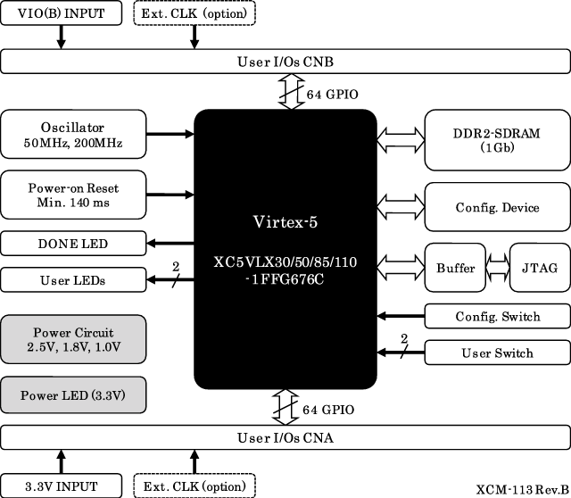
Xcm 113 Xilinx Virtex 5 Ffg676 Fpga Board

Virtex 6 Block Diagram Wiring Diagram G9

The Wfm Data Handling Unit Architecture Centered On The
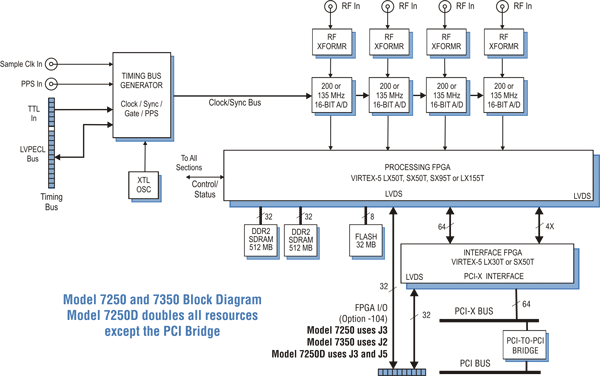
Pentek Model 7656
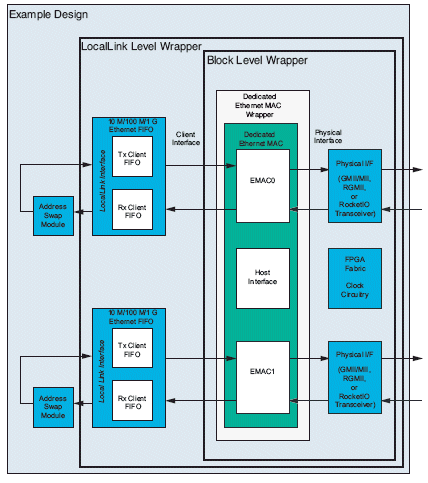
Designing With Virtex 5 Embedded Tri Mode Ethernet Macs

Fm485 Virtex 5 Pmc Xmc 4dsp Llc
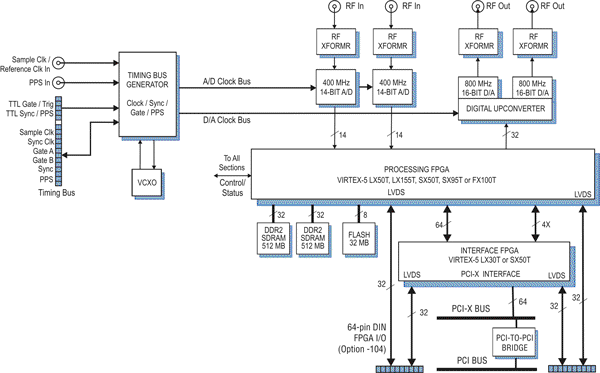
Pentek Model 7250

Simplified Structure Of Xilinx Virtex 5 Fpgas Download
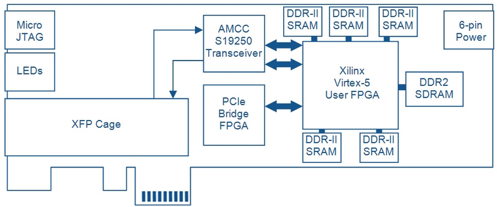
Nallatech 180 Virtex 5 Lx155 Xfp Port 10 Gbe And Oc192

Power Supply Solutions For Xilinx Fpgas
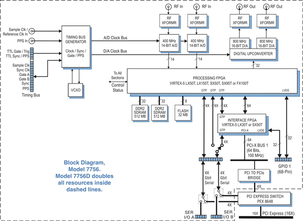
Pentek Model 7756

Xps Usb 2 0 Host Controller

Adm Xrc 5t2 Adv Xilinx Virtex 5 Fpga Pmc And Jpeg2000

Figure 4 1 From Implementation Of Ethernet Aurora And
